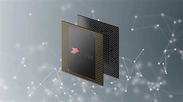
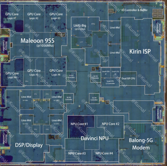
A die shot of HiSilicon’s Hi36E0 chip has provided physical evidence for Huawei’s LogicFolding architecture: the Kirin 9050 Pro package contains two vertically stacked silicon dies, separating logic from SRAM and cache. The image, published by Kurnal Insights, confirms that the design is more than a presentation concept, although it does not by itself establish how the chip compares with the fastest processors made on leading-edge nodes.
Kurnal Insights identifies the arrangement as dual-die Logic + SRAM stacking. Each die measures 11.13 × 10.84 mm, or roughly 120.65 mm². Rather than placing all processing and memory circuitry across one planar die, Huawei has positioned a dedicated SRAM/cache layer above the logic layer.
Huawei says the approach increases equivalent transistor density from about 155 million to 238 million transistors per mm², a 55% gain. The company also cites around 5 million inter-die connections, 125 TB/s of bandwidth between the layers, and a 30% reduction in latency on critical paths.
- Equivalent transistor density: about 238 million transistors per mm², up from about 155 million
- Inter-die connections: approximately 5 million
- Inter-die bandwidth: up to 125 TB/s
- Claimed critical-path latency reduction: 30%
Stacking SRAM closer to the logic that needs it can shorten data paths without requiring every part of the design to move to a newer manufacturing process. That matters for Huawei and SMIC, which do not have access to the same leading-edge fabrication nodes used by TSMC for processors from Apple, Qualcomm and MediaTek. The trade-off is more demanding bonding, alignment and packaging work, especially with millions of connections crossing the two layers.
The Kirin 9050 Pro has already appeared in Huawei’s Mate 90 lineup. Huawei lists the chip in the Mate 90 Pro Max and Mate 90 RS, with a nine-core CPU supporting 16 threads. Relative to the prior generation, Huawei claims 23% higher multi-core CPU performance, 40% higher GPU performance and a 140% NPU increase.
Reports circulating in industry sources have suggested that the logic die uses SMIC’s N+3 process while the SRAM layer uses N+2. Kurnal Insights confirms the two-die structure and SMIC manufacturing, but its public report does not separately assign those process labels to the individual layers, and Huawei has not officially confirmed them. The exact process split therefore remains unresolved.
The die shot verifies the basic vertical construction behind LogicFolding, but independent performance, power-efficiency and manufacturing-yield analysis will be needed to judge how far the design closes the gap with processors built on the industry’s most advanced fabrication processes.