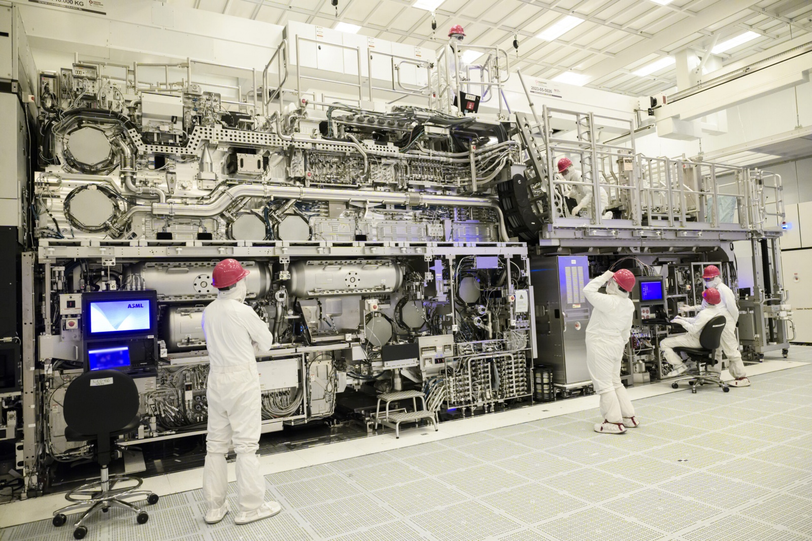
Samsung plans to bring ASML’s High-NA EUV lithography into volume DRAM production in 2028, extending a partnership aimed at manufacturing denser and more advanced memory chips. The technology could reduce the number of manufacturing steps needed for finer circuit patterns, potentially improving efficiency over time.
EUV lithography uses extreme ultraviolet light to transfer circuit designs onto silicon wafers. High-NA EUV adds a more capable optical system, enabling finer details than current EUV tools. For Samsung, the immediate target is DRAM, the high-speed memory used across smartphones, PCs, graphics hardware and data-center servers.
The move does not mean devices released in 2028 will automatically receive dramatically higher RAM capacities or battery-life gains. High-NA EUV is a factory technology rather than a consumer-facing feature, but more precise manufacturing can support smaller, denser and potentially more power-efficient future memory generations for mobile devices, PCs and AI accelerators.
Samsung is also participating in an initiative for 12-inch photomasks, the templates used to transfer circuit patterns during chip production. The industry has long relied on 6-inch masks, while High-NA EUV systems expose a smaller area in a single pass. On larger chips, that can require separate exposures to be aligned through a process known as stitching.
Larger 12-inch masks are intended to make High-NA EUV more efficient for large chips by reducing the need for such stitching and its associated cost. The expanded work also aligns with Samsung’s preparations for 1.4 nm semiconductor manufacturing, where High-NA EUV is expected to be an important production technology.
Samsung’s 2028 DRAM goal places the company among chipmakers preparing the next major lithography transition as demand rises for advanced memory and processors. The key remaining question is how quickly High-NA EUV can scale economically beyond initial deployments and into broad high-volume manufacturing.