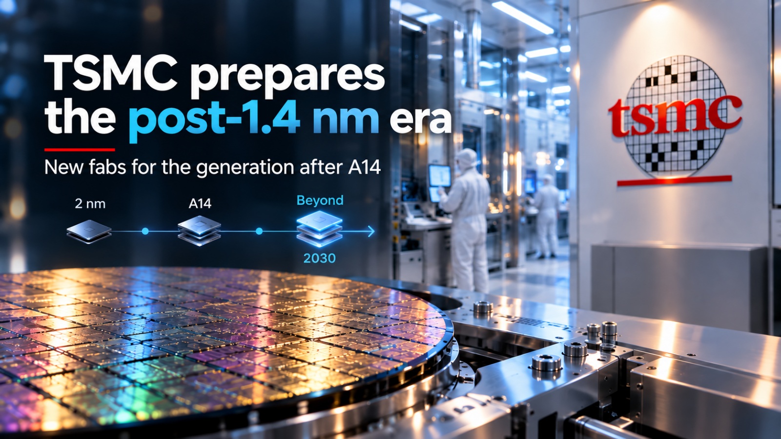
TSMC has secured approval to expand its Longtan Phase 3 project, laying the groundwork for three fabrication plants designed to produce chip technologies beyond the company’s A14 process. The first facility is targeted to begin production around 2030, underscoring how far ahead advanced-node capacity must be planned.
The company has not disclosed the commercial name or technical specifications of the process intended for the new fabs. The development is therefore an infrastructure commitment rather than an announcement of a finished sub-1.4nm manufacturing node.
TSMC is currently manufacturing chips on its N2, or 2nm, family. Its next major step is A14, which is scheduled for volume production in 2028 and uses a new generation of gate-all-around nanosheet transistors. In this design, the gate controls the transistor channel from multiple sides.
- For A14 versus N2, TSMC projects 10% to 15% higher performance at the same power.
- For A14 versus N2, TSMC projects 25% to 30% lower power consumption at the same performance.
- TSMC also projects more than a 20% increase in logic density for A14 compared with N2.
Those gains could enable faster mobile silicon without a matching increase in power draw, or similar performance with lower energy consumption. Higher logic density is also important for large server processors and AI accelerators, where more circuitry can fit within the same silicon area.
The technologies after A14
| Time frame | TSMC technology | Reported change |
|---|---|---|
| 2025-2026 | N2 / 2nm | First nanosheet generation |
| 2028 | A14 | Higher density, lower power use and higher performance |
| 2029 | A13 / A12 | Area and power-delivery refinements |
| Around 2030 | Post-A14 processes | More advanced technologies for the Longtan fabs |
As chip designs become denser, shrinking transistors is only part of the challenge. Power routing increasingly competes with signal wiring for space in the chip’s metal layers. TSMC’s answer for upcoming generations is Super Power Rail, a backside power-delivery approach that moves part of the power network to the rear of the wafer, leaving signal routes less congested.
The approach is particularly relevant to very large processors and AI accelerators, which must supply power to billions of transistors simultaneously. Reduced interconnect congestion can potentially improve both power efficiency and operating frequencies.
Building a leading-edge fab requires years of work on land, power, ultrapure water, clean-room facilities and lithography equipment before volume manufacturing begins. The Longtan approval gives TSMC time to prepare capacity for the process family that follows A14.
Intel is also targeting its 14A process for 2028, with gate-all-around transistors and advanced power delivery. The next phase of foundry competition will depend on transistor architecture, power routing and interconnect density as much as the node label. TSMC’s exact post-A14 process and the technology that will enter the Longtan fabs remain undisclosed.