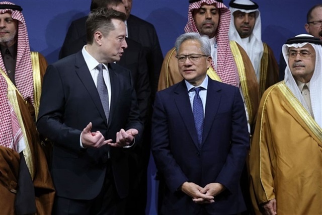
China could reach advanced lithography by 2030, according to Nvidia CEO Jensen Huang, a timeline that would materially strengthen the country’s semiconductor self-sufficiency. Elon Musk has offered an even shorter two-to-three-year estimate for China to address broader constraints in computing capacity, lithography and chip manufacturing.
Speaking at the All-In Summit, Huang was asked when China might develop its own advanced lithography systems. His 2030 estimate was framed around China’s ability to turn working technology into high-volume manufacturing, rather than around a specific announced machine. In an interview with China Media Group, Musk said Chinese AI models are already producing strong results relative to the computing resources available to them, and argued that domestic lithography and semiconductor development could rapidly ease the hardware bottleneck.
Advanced lithography is not necessarily ASML-class EUV
The forecasts should not be read as a firm prediction that China will have an ASML-equivalent extreme ultraviolet lithography machine by 2030. Huang referred to “advanced lithography,” a wider category that can include deep ultraviolet immersion systems and manufacturing techniques that extend older equipment to more advanced process nodes.
China has made progress with DUV immersion lithography. SMIC has shown that DUV equipment can be pushed toward advanced nodes through multiple patterning, though the approach adds process complexity, slows production and raises costs compared with EUV-based manufacturing.
A Chinese EUV effort is also under way. A prototype reportedly built with help from former ASML engineers was able to generate EUV light, but had not yet manufactured chips. Moving from a laboratory demonstration to high-yield production of millions of chips remains a substantially harder step.
The gap between different forecasts reflects different technical thresholds. Frank Rohmund, head of Zeiss Semiconductor Manufacturing Technology and formerly responsible for the company’s EUV business, has estimated that China could need about 15 years to develop its own EUV systems. Zeiss supplies the specialized optical systems essential to ASML’s EUV machines.
Meanwhile, ASML’s target is advancing. The company is considering output of more than 110 Low-NA EUV systems in 2028, following at least 80 planned for 2027, driven largely by AI-chip capacity expansion. ASML has also demonstrated a 1,000-watt EUV source, up from 600 watts, and is targeting productivity of up to 330 wafers per hour by 2030.
EUV exports to China have been restricted for years, with controls also expanding to certain advanced DUV tools. Those limits have intensified investment in domestic semiconductor capabilities across China’s chip ecosystem, including Huawei and SMIC. Even without copying ASML system for system, locally developed equipment that is capable enough for domestic fabs could reduce the practical impact of those restrictions.
China may plausibly have far more capable domestic lithography by 2030. The unresolved question is whether that progress will amount to a workable alternative for local chip production or true parity with ASML’s continually advancing EUV platform.